Structural Characterization of InSe and InSe:Cu Binary Semiconductors Growing Using Bridgman/Stockbarger Technique and Effect of Copper
Received Date: August 14, 2024 Accepted Date: September 14, 2024 Published Date: September 17, 2024
doi:10.17303/jmsa.2024.8.105
Citation: Bekir Gürbulak, Songül Duman, Fikriye Şeyma Kaya (2024) Structural Characterization of InSe and InSe:Cu Binary Semiconductors Growing Using Bridgman/Stockbarger Technique and Effect of Copper. J Mater sci Appl 8: 1-10
Abstract
The study of semiconductors has been going on for a century. The growth, research and development of single crystals is of great importance to the advancement of semiconductor technology. The fact that research on these binary crystals can find many applications in technology encourages researchers to work on this subject. Binary semiconductors are used in visible and infrared light-emitting diodes, infrared detectors, converters, amplifiers, optical parameter oscillators and far-infrared generators, as well as in the generation and recording of optical signals. Indium and selenium have been synthesised from high purity elements (at least 99.999%) in stoichiometric ratios. InSe and InSe:Cu single crystals were successfully grown by the modified Bridgman/Stockbarger crystal growth method with a doping of three tenthousandths of copper. Since the ingots of the grown crystals have a layered structure, samples were easily prepared along the (001) planes. The most characteristic feature of the III-VI layered semiconductor family is that it is layered. As the surface areas of the grown samples did not contain any impurities, they were not subjected to any further chemical treatment. The structure of the InSe and InSe:Cu semiconductors was analysed using X-ray diffraction (XRD), scanning electron microscopy (SEM) and energy dispersive x-ray (EDX) techniques.
Keywords: Grown; InSe; InSe:Cu; Bridgman/Stockbarger Method; Structural Characterization
Introduction
Although AIIIBVI, AIVBVI and AIIBVI compounds have been studied for many years, the study of AIIIBVI type compounds has started recently. Great advances have been made in semiconductor technology by growing and researching such crystals. Binary semiconductors have a great importance and contribution to the development of nanotechnology. Growing semiconductors cheaply, easily and with high quality will increase their application areas. To increase the application area of binary semiconductors, it is necessary to determine the structural, optical, electrical and magnetic properties of the sample. III-VI semiconductors have garnered significant interest due to their unique electrical and optical properties, as well as their potential applications in electronic and optoelectronic devices. Numerous studies have been conducted to explore these characteristics [1-4].
Indium selenide (InSe) is a layered semiconductor that can be split to yield high-quality surfaces. Scientific studies have shown that it belongs to a new class of materials with attractive properties for solar energy conversion applications. Some properties of InSe across layers have been widely investigated in recent years [5-9]. The crystals are made of a fourfold stacking of selenium-indium-indium and selenium atom sheets which characterize all M2X2 molecular-like crystals.
The Bridgman-grown crystals usually belong to the modification; their unit cells are rhombohedral and extend over three layers [10]. InSe belongs to a large class of layered semiconductors in which a prototype of covalent or ionic forces extends in two dimensions instead of being three-dimensionally bonded as in group III–VI, IV or III–V semiconductors [11]. Large InSe single crystals have been grown by the Bridgman-Stockbarger method, starting from stoichiometric and non-stoichiometric melts [12].
X-ray diffraction measurements revealed that the Cd-doped InSe semiconductor grows in a hexagonal structure, with unit cell parameters a=b=4.00 Å and c=16.63 Å. Doping significantly alters the structural, electrical, and photoconduction properties of thermally evaporated polycrystalline p-type α-In2Se3 thin films. The layered hexagonal structure of the α-In2Se3 phase transforms into a layered hexagonal InSe monophase upon Cd doping. Cd doping into the semiconductor caused observed changes in unit cell parameters, reflection lines and stacking patterns [13].
There are few studies available on the impurity levels in p-type InSe, with only group II elements Zn and Cd being used as dopants [14]. Investigations into the impurity levels in Zn and Cd-doped InSe have employed deep level transient spectroscopy (DLTS), photoluminescence (PL), and Hall-effect measurements. The 1.17 eV emission band observed in the Zndoped sample can be explained by a self-activated luminescence process, which is described by a configurational coordinate model [14].
InSe single crystal ingot has been enlarged to 12 mm in diameter and approximately 80 mm in length. These ingots exhibited no cracks or voids on their surfaces. Absorption measurements were conducted for InSe sample within a temperature range of 10–320 K. The binding energy of InSe was determined to be 20.5 meV. The direct band gap of InSe was estimated to be 1.339 eV at 10 K, 1.289 eV at 200 K, and 1.256 eV at 300 K [15]. InSe belongs to the broad class of layered semiconductors. It has a significant anisotropy of chemical bonds within and between layers. This allows the preparation of natural preparations. Having an energy band gap of 1.2-1.3 eV, sensitivity to sunlight, mobility of carriers and diffusion length in the layer encourages the search for the optimal heterostructure based on InSe for solar elements and other photoelectric sensors [16-18].
The aim of this study is; first, to grow pure InSe and doped InSe:Cu binary semiconductors using the BridgmanStockbarger method. The second is; to examine the structural changes caused by the doped copper (Cu) element on the InSe compound.
Growth and Structural Characterization
The Bridgman-Stockbarger method is a widely used growth technique for growing semiconductors. The Bridgman-Stockbarger method is an improved version of the Bridgman method and provides growth in a controlled environment. It is very important to grow binary compounds and to ensure that the grown semiconductor is of quality to be used in scientific studies. Considering the studies [19,20], it was decided to grow InSe and InSe:Cu crystals using a single ampoule. The melting point of the InSe compound, determined from the phase diagram, was determined to be 660±5 °C [20,21]. Growth and structural characterizations of single crystals like InSe and InSe:Cu typically involve several steps and techniques. Indium, selenium copper is supplied in high purity. Indium and selenium are formed in proportions obtained by stoichiometric calculations. Three ten thousandths of Cu are added to this mixture. A growth ampoule is prepared from a quartz pipe with an inner diameter of 12 mm and a length of 50 cm. The lower end of the growth ampoule is shaped according to the layered structure and the elements In and Se (doped: Cu) are placed inside the ampoule. The air in the growth ampoule was reduced to 10-6 Torr and the tip of the ampoule was sealed under vacuum. The mixture is slowly melted in a controlled environment under a vacuum inside the growth furnace. The alloy formed inside the quartz bulb is heated to 30-50 C above the melting temperature. During the formation of the compound, the temperature and cooling rate are carefully controlled.
For the pre-reaction, the component elements prepared in stoichiometric proportions were sealed in the growth ampoule. The grown ampoules were placed in a cage designed from kanthal DSD-Cr-Al-Fe alloy wire. It is fixed to the shaking furnace by means of connection wires made from both ends of the cage at an appropriate distance determined parallel to the furnace pipe. The reaction process, which is the first step of the crystal growth process, has started. Considering that indium would react and melt selenium as a result of the thermal conductivity in the InSe: The reaction between In and Se was initiated by ensuring that indium was above its melting temperature (Inm.t: 157 C) and selenium was below its melting temperature (Sem.t: 217 C). This will prevent the sudden increase in temperature and pressure inside the ampoule. After being kept at the specified temperature for 50 minutes, it was increased to 217 C within 60 minutes and kept at this temperature for 2 hours. Since the exothermic reaction between In and Se continues at 217 C, a long time is needed to eliminate risks such as explosion or cracking of the ampoule. Since the vapour pressure of selenium is high between 600 C and 950 C, the lower and upper zone temperatures of the crystal growth furnace were increased to 500 C, respectively, within 20 hours and kept at 500 C for 12 hours. Then, it increased from 500 C to 850 C in 30 hours and remained constant at this temperature for 20 hours. Then it was reduced to 30 C in 52 hours. As a result of the preliminary reaction, the vapour pressure of the alloy was reduced and explosion or cracking problems in the next growth step were tried to be minimized.
The second step of the crystal growth process, the growth process, has started. It was considered that the In, Se and Cu mixture would increase the vapour pressure of selenium by entering into a chemical reaction as a result of thermal conductivity. The lower and upper zone temperatures of the growth furnace were increased to 600 C within 10 hours. It was kept at 600 C for 15 hours. Since the exothermic chemical reaction between the elements In, Se and Cu continues at 650 C, a long period is needed to eliminate risks such as explosion and cracking of the ampoule. Again, the alloy was heated to 1000 C for 20 hours and waited for 10 hours. To ensure homogeneous distribution of In, Se and Cu elements, the mixture was shaken by moving the ampoule up and down at an angle of approximately 45° for 5 hours. The growth furnace is fixed at an angle of 60-70° to the horizontal.
The upper zone temperature of the crystal growth furnace was first kept constant at 1000 C for 50 hours. Then it was reduced to 800 C for 80 hours and the temperature was kept constant at 800 C for 50 hours. 60 hours at 650 C, 40 hours at 250 C, and 10 hours at 30 C. The furnace lower zone temperature was reduced to 800 C in 50 hours, 650 C in 50 hours, 250 C in 40 hours, 100 C in 10 hours and 30 C in 10 hours, and the furnace was turned off.
Thus, using the same growth temperature program at the same time, the growth process of InSe and InSe:Cu binary semiconductor crystals was completed in approximately 6 to 21 days, including the reaction. At the end of the growth process, the compounds were removed from the growth oven. The ampoules were cut with the help of a suitable cutter to prevent the ingot semiconductors from suffering any hardness or deformation. The ingot must be stored in a very clean environment to prevent chemical contamination of the samples [20,22,23]. This process is important so that semiconductors can be used in certain optical, electrical and magnetic applications. Therefore, it is important to apply and perform this method carefully. Many scientists have grown InSe single crystal using the Bridgman method and examined its various parameters [24-26].
Experimental
In our crystal growth laboratory, pure, copper doped (0.03%) elements were weighed to grow InSe single crystals using the modified Bridgman-Stockbarger method. The first basic step in obtaining high quality crystals for the polycrystalline A IIIB VI component is that the basic elements in the structure are 6N pure. These elements were weighed to a precise stoichiometric ratio down to 0.01 mg. The total mass of the elements was determined to be approximately 60 grams. The basic criteria for this choice were, firstly a sufficient need to justify the cost of one run, secondly minimal loss of the material in case of breakage. This stoichiometric ratio necessary to produce 60 g InSe was calculated using the following relationships:
with total mass,
where, M and A are total and atomic masses, respectively [20].
An attempt was made to grow InSe single crystals by providing the basic elements In and Se with a purity of approximately 99.999%. Chemical elements were weighed to a precise stoichiometric ratio down to 0.01 mg. The total mass of the elements is standardized to 60 g. The stoichiometric composition of the source material was determined to be approximately 52% In and 48% Se. Bulk InSe crystals have been grown in our crystal laboratories using the horizontal Bridgman Stocbarger method. The samples were obtained by cutting the ingot parallel to the layers with a razor blade.
X-ray diffraction patterns of InSe and InSe:Cu binary compound are shown in Figures 1a and b. has been given. Figure 2b. The effect of doping Cu elements on the InSe semiconductor on the crystal is clearly seen in Figure 1b. Interplane distance dhkl (table 1) was calculated from the XRD data using the Bragg relationship.
Results and Discussions
The modified Bridgman Stockbarger method is a technique used in the crystal growth process. This method occupies an important place in the production of high-quality and large crystals and has a wide range of applications in materials science, semiconductor industry and optics. Basically, the material planned to be grown is prepared to high purity and placed in a growth vessel or a container containing the solution. It is heated to create a controlled temperature gradient. The growth bulb is placed in the designated area of the two-zone oven. Taking into account the melting temperature and phase transitions of the semiconductor, the furnace temperature is gradually reduced very slowly by creating a temperature gradient in both regions. In this process, a crystal structure is formed during the transition from melt to solid.
The first important step in obtaining high quality crystals is the purity of the main materials in the structure. An attempt was made to grow InSe single crystals by supplying the basic elements In and Se with a purity of approximately 99.999%. Chemical elements were weighed to a precise stoichiometric ratio down to 0.01 mg. The total mass of the elements is standardized to 60 g. The main criteria for this selection were, first of all, the cost of a single operation, sufficient need and minimum material loss in the form of cracking of the growth bulb were taken into account. The elements to be used in growth (Cu, In and Se, etc.) were used in high purity (99.999%) pieces with a particle size of approximately 2 mm. The elements were weighed and loaded into a thick-walled growth ampoule. Quartz bulbs were sealed with a torch under a pressure of approximately 10-6 Torr. The stoichiometric composition of the source material was determined to be approximately 52% In and 48% Se. Bulk InSe crystals have been grown in our crystal laboratories using the horizontal Bridgman-Stocbarger method. For this purpose, InSe and InSe:Cu semiconductors were grown with the modified Bridgman/Stockbarger technique developed in our current crystal growth laboratory. XRD spectra of InSe and InSe:Cu semiconductors were taken by preparing a 50-60 micron thick sample parallel to the layers using nonmetal tweezers.
The crystallographic parameters of the InSe and InSe:Cu crystal structure were determined. The resulting InSe binary compound is a blackish crystal. X-ray diffraction patterns of InSe and InSe:Cu binary compound are shown in Figures 1a and b. The XRD spectra do not contain any impurity phase lines. The unit cell parameters of the InSe semiconductor were obtained as a = 4.04 Å and c = 16.730 Å. Comparison of the XRD patterns of InSe and InSe:Cu revealed their compatibility with each other. The structures of InSe and InSe:Cu compounds are almost equal.
Structural characterization of InSe and InSe:Cu compounds, an attempt was made to explain it with the help of XRD, SEM measurements and energy distribution analysis of X-rays. If the percentage of Cu doping is appropriate, the XRD spectra of InSe single crystals increase and become sharper. For doping levels above 0.3%, Cu atoms are predominantly localized between layered packs and can form localized states. In this way, charge carriers recombine intensively. This situation was observed in our study.
As shown in Figure 2, the XRD peaks in the Cu-doped samples are sharper than those in the undoped sample. The effect of doping Cu elements on the InSe semiconductor is seen in Figure 2. The increase in peak level may be due to the reduction of impurities in the pure material through Cu doping. This can be expected due to the roles of Cu atoms in InSe. The results show that InSe single crystals contain many impurities and they are eliminated by doping with Cu.
The doping process removes impurities between layers and is thought to neutralize existing impurities by forming complexes. Interplane distance dhkl (table 1 and 2) was calculated from the XRD data using the Bragg relationship.
Using the Bridgman-Stockbarger method, he grew stoichiometric and non-stoichiometric InSe single crystals and made structural analysis of the crystals with the help of electron microscopy. It was stated that the grown crystal had a hexagonal structure [12]. Experimental studies were carried out by preparing 50-60 nm thick samples for SEM and EDX from InSe and InSe:Cu ingots, which have a hexagonal structure.
Surface morphology images of InSe and InSe:Cu crystals were obtained by scanning electron microscope (SEM) technique at 15 kV with a magnification of 25,000. The surface of InSe and InSe:Cu compounds was coated with gold to clarify the SEM images. Figure 3 shows the SEM images of undoped InSe and InSe:Cu crystals. It is seen that InSe and InSe:Cu semiconductors have very smooth and homogeneous surfaces.
Figures 4a and b. Figure 4a and b. EDX data of InSe and InSe:Cu semiconductors grown at room temperature are given. According to EDX results, InSe and InSe:Cu contain In = 55.88%, Se = 38.84%, and O = 5.28% and InSe:Cu, In = 56.77%, Se = 38.38% and O = 4.84%, respectively. The EDX spectrum of InSe crystal was found to be very close to that of InSe:Cu crystals. It has been observed that the Cu effect creates a more homogeneous and high-quality structure in InSe crystal. It was determined that the grown InSe and InSe:Cu semiconductors had high quality stoichiometric ratios and homogeneous surfaces. These values are very close to the expected values, and it is predicted that some In bonds with O. Results similar to those obtained from EDX analyses have been observed in many studies [27].
The crystallization of microstructures formed at different growth stages was analysed using XRD. Figure 1 shows the XRD pattern. The θ-2θ scan data corresponding to the (002), (004), (006) and (008) (0012) and (0014) diffraction planes of the InSe and InSe:Cu semiconductor were 11.20, 21.92, 32.95, 44.08, 68.07 and 81.42 exhibits peaks, respectively. The approximate lattice parameters of InSe and InSe:Cu semiconductor (a = b = 4.04 Å and c = 16.730 Å) were found to be comparable to other scientific studies. Although the intensities of the XRD spectra of the InSe:Cu binary compounds increased compared to the spectra of the InSe compound, no new noticeable peaks were formed due to impurities.
In conclusion; InSe and InSe:Cu semiconductor ingots were grown to 10 mm in diameter and approximately 70 mm in length. No cracks or voids were observed on the surfaces of the ingots. Since there were naturally no scratches, cracks or contamination on the surfaces of the grown InSe and InSe:Cu samples, no additional cleaning process was required. Experimental studies of XRD, SEM and EDAX measurements play a key role in gaining scientific information about the structural properties and potential applications of InSe and InSe:Cu single crystals. Determining the structural characterization of layered single crystals is crucial for optimizing them for applications in solar cells, photodetectors, and other optoelectronic devices.
Acknowledgements
This work ''FYL-2023-10176, Project ID: 10176 Structural Characterization of XIIIn2Se4 (XII: Cu, Mn Fe, Ni, etc.) Ternary Semiconductors Grown by Bridgman/Stockbarger Technique,'' was supported by Atatürk University BAP (Scientific Research Projects).
- Yoshida Ye JT, Nakamura Y, Nittono O, (1995) Appl. Phys. Lett.
- Zubiaga A, Garcia JA, Plazaola F, Munoz-Sanjose V, Martinez-Tomas C, (2003) Phys. Rev. B.
- Homs AA, Mari B, (2000) J. Appl. Phys.
- Gürbulak B, (2004) Phys. Scripta. 70: 197.
- De Blasi C, Micocci G, Rizzo A, Tepore A, (1982) Phys. Status Solidi A 74: 291.
- Segure A, Pomer F, Cantarero A, Krause W, Chevy A, (1984) Phys. Rev. B 29: 5708.
- Tagiev BG, Niftiev GM, Sn. Aidaev F, (1985) Phys. Status Solidi A 89: 639.
- Segure A, Mari B, Martinez-Pastor J, Chevy A, (1991) Phys. Rev. B 43: 4953.
- Riera J, Segure A, Chevy A (1993) Phys. Status Solidi A 136: K47.
- Camassel J, Merle P, Mathie H, Chevy A, (1978) Phys. Rev. B 17: 4718.
- Abd El-Moiz AB, (1993) Physica B 191: 293.
- De Blasi C, Micocci G, Mongelli S, Tepore A,(1982) J. Cryst Growth 57: 482.
- Qasrawı AF, (2002) Cd-Doping Effects on The Properties of Polycrystalline α-In2Se3 Thin Films, Cryst. Res. Technol. 37: 378-90.
- Ikari T, Shigetomi S, Koga Y, Shigetomi S, (1981) phys. stat. sol. (b) 103: K81.
- Gürbulak B, Yıldırım M, Ateş A¸ Doğan S, Yoğurtçu YK, (1999) Growth and Temperature Dependence of Optical Properties of Er Doped and Undoped n-Type InSe, Jpn. J. Appl. Phys. Part 1, No. 9A, 38: 5133-6.
- Siciliano T, Tepore A, Micocci G, Genga A, Siciliano M, Filippo E, (2011) Formation of In2O3 Microrods in Thermal Treated InSe Single Crystal, Cryst. Growth Des. 11: 1924-9.
- Katerynchuk VN, Kovalyuk MZ, (1992) J. Tech. Phys. Lett. 18: 70.
- Segura A, Guesdon JP, (1979) Besson J.M., Chevy A., Rev. Phys. Appl. 14: 253.
- Shih I, Champness CH, Shahidi AV, (1986) Growth by Directional Freezing of CuInSe2 and Diffused Homojunctions in Bulk material. Solar Cells, 16: 27-41.
- Gürbulak B, (1997) PhD Thesis, Atatürk University, Türkiye.
- Imai K, Suzuki K, Haga Ti, Haegawa Y, Abe Y, (1981) Phase diagram of In-Se system and crystal growth of indium monoselenide. Journal of Crystal Growth, 54: 501.
- Gürbulak B, Duman KA, Dumanlı MK, (2023) Structural Characterization XIn2Se4 Ternary Semiconductors Grown with Bridgman/Stockbarger Technique, Atatürk University Journal of Anatolian Physics and Astronomy (ISSN: 2791-8718) 1: 77-85.
- Bodnara IV, Viktorov IA, Pavlyukovets SA, (2010) Growth, Structure and Thermal Expansion Anisotropy of FeIn2Se4 Single Crystals, Inorganic Materials, 46: 604-8.
- Chevy A, Kuhn A, Martin MS, (1977) Large InSe monocrystals grown from a non-stoichiometrik melt. J. Crys. Growth, 38: 188.
- Tagiyev BG, Nitfiyev GM, Aidayev F Sh, (1985) Photoluminescence and photoconductivity of indium selenide single crystals doped with rare-earth elements. Solid State Communications, 53: 877-9.
- Lukyanyuk LV, Voronyuk SP, Kovalyuk ZD, (1989) Alkali-metalintercalated indium and gallium selenides. Phys. Stat. Sol. (b) 155: 717.
- Viswanathan C, Gopal S, Thamilselvan M, Premnazeer K, Mangalaraj D, Narayandass SK, Yi J, (2004) Journal of Materials Science: Materials in Electronics, 15: 787-92.
FIGURE 1
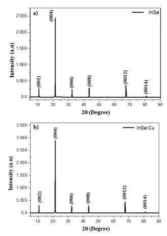
Figures 1a and b: XRD spectra of InSe and InSe:Cu binary compound are given at room temperature. Miller indices are shown at each diffraction peak
FIGURE 2
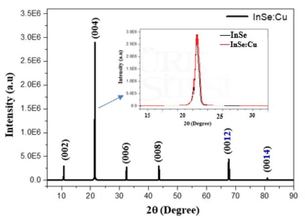
Figure 2: The effect of doping the Cu element on the InSe semiconductor on the peak intensity
FIGURE 3
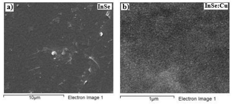
Figure 3: SEM images taken at 15 kV with a 25.000 magnification for (a) InSe and (b) InSe:Cu crystals
FIGURE 4
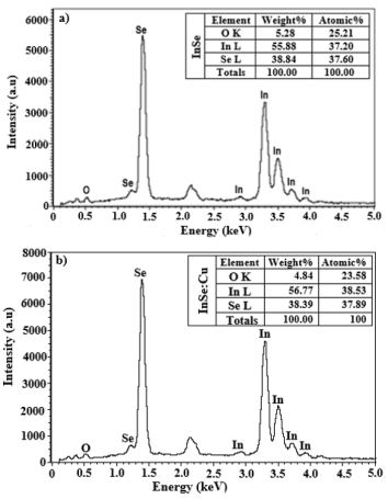
Figures 4a and b: EDX data of a) InSe and b) InSe:Cu crystal grown at room temperature
Tables at a glance
Figures at a glance