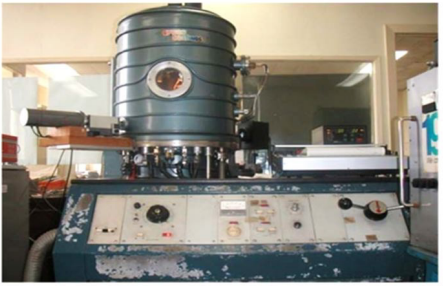
Figure 1: Experimental setup of thermal evaporation system
Figure 1: Experimental setup of thermal evaporation system
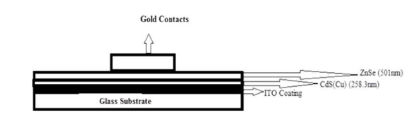
Figure 2: Methodology for Multilayer of CdS(Cu)/ZnSe on ITO coated substrate
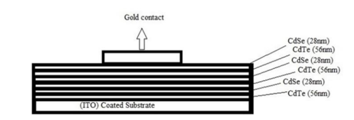
Figure 3: Methodology for Multilayer of CdTe/CdSe on ITO coated substrate

Figure 4: Methodology for Multilayer Deposition through Thermal Evaporation Technique
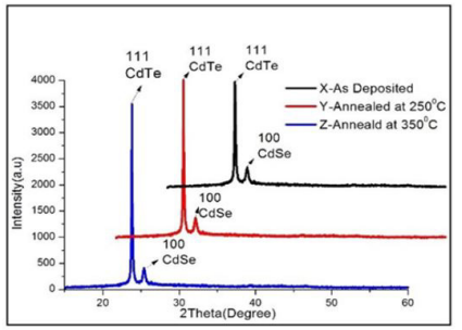
Figure 5: Combined graph of XRD spectra of all samples X, Y, and Z
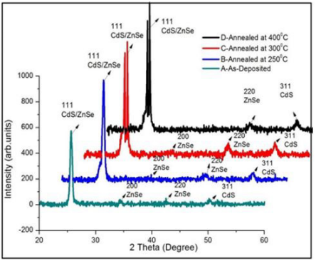
Figure 6: Combined graph of XRD spectra of all samples A, B, C and D
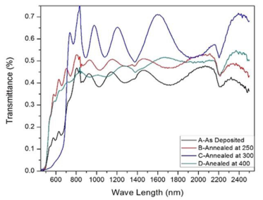
Figure 7: CdS (Cu)/ZnSe samples' transmission spectra at 250, 300, and 400 degrees Celsius after annealing.
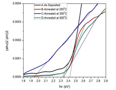
Figure 8: Band gaps of all the samples of CdS (Cu)/ZnSe annealed at 250, 300, and 400oc
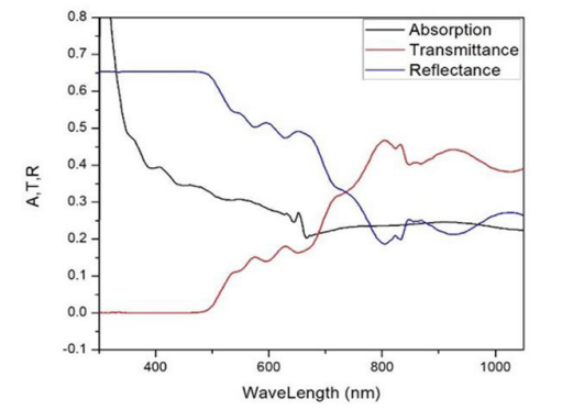
Figure 9: Absorption, transmittance and reflectance spectra as a function of wavelength of ZnSe thin film
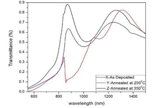
Figure 10: Transmission graph of all the samples of CdTe/CdSe multilayer heterostructure X, Y and Z
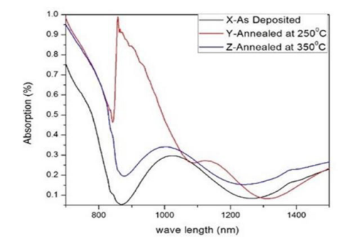
Figure 11: Absorption spectra of all the samples of CdTe/CdSe X, Y and Z
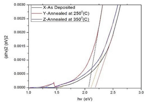
Figure 12: Bandgap of multilayer heterostructure of X, Y, and Z
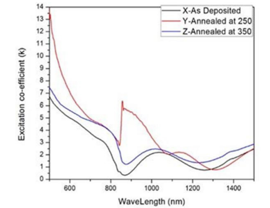
Figure 13: Extinction coefficient of CdTe/CdSe multilayer heterostructure.
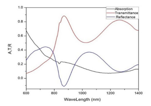
Figure 14: Absorption (A), transmittance (T) and reflectance (R) spectra as a function of wavelength of CdTe/CdSe multilayer
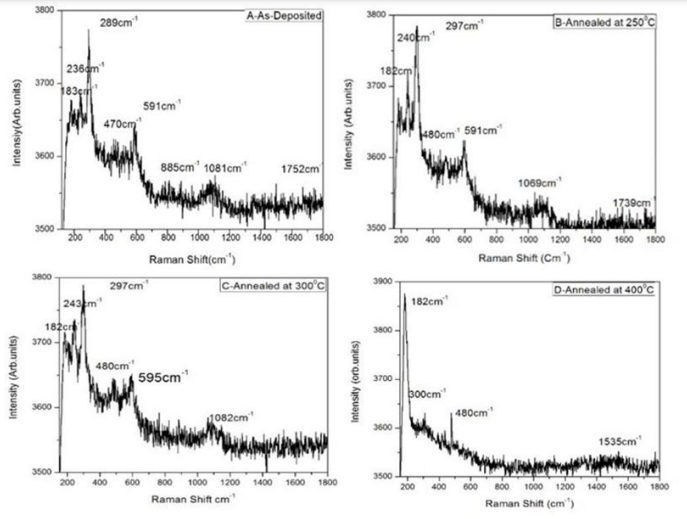
Figure 15: Raman spectra of CdS (Cu)/ZnSe multilayers annealed at 2500C, 3000C, 4000C and as deposited

Figure 16: Raman shift of CdS (Cu)/ZnSe multilayer heterostructure vs annealing temperature
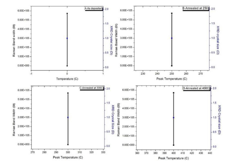
Figure 17: Raman Bandwidth/crystal size graph of multilayer heterostructure of CdS (Cu)/ZnSe
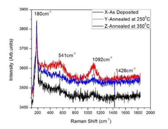
Figure 18: CdTe/CdSe Multilayer heterostructure Raman spectra
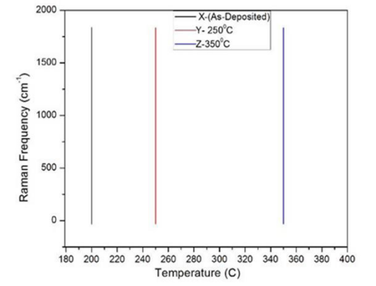
Figure 19: Raman shift vs annealing Temperature of CdTe/CdSe multilayer heterostructure
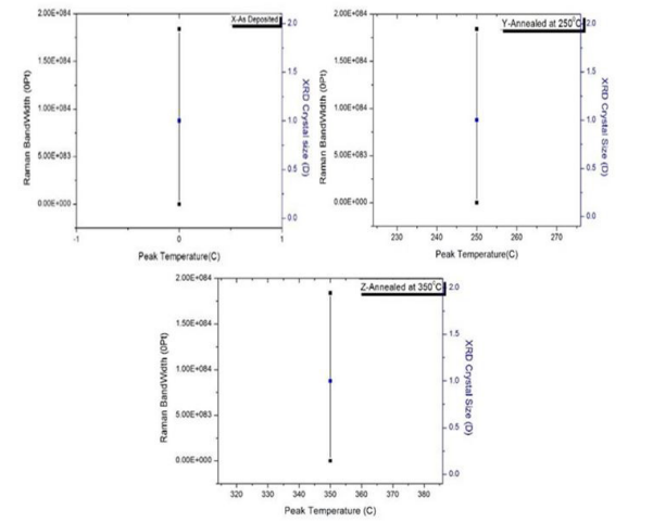
Figure 20: Raman Bandwidth/crystal size graph of CdTe/CdSe multilayers
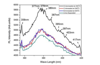
Figure 21: PL emission spectra of CdS (Cu)/ZnSe multilayer heterostructure
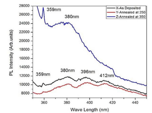
Figure 22: PL Emission spectra of CdTe/CdSe multilayer heterostructure
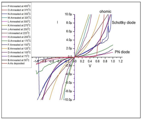
Figure 23: The IV characteristics PN junction of CdS (Cu)/ZnSe
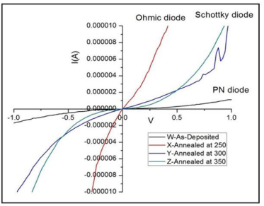
Figure 24: The IV characteristics PN junction of CdTe/CdSe
Tables at a glance
Figures at a glance