Hydrogen Gas Sensor Based on CuO and Pd-doped CuO Thin Films Grown by sol-gel Spin Coating Method
Received Date: March 08, 2025 Accepted Date: April 08, 2025 Published Date: April 011, 2025
doi:10.17303/jmsa.2025.9.101
Citation: Mohamed Jlassi, Mehdi Dhaouadi, Imen Sta, Michael Kompitsas (2025) Hydrogen Gas Sensor Based on CuO and Pd-doped CuO Thin Films Grown by sol-gel Spin Coating Method. J Mater sci Appl 9: 1-13
Abstract
In this work, hydrogen sensors were demonstrated based on copper oxide (CuO) and palladium-doped copper oxide (CuO:Pd) thin films grown by sol-gel spin coating technique. The sensing properties of CuO layer surfaces were analyzed for hydrogen concentrations varying from 1000-15000 ppm in a temperature range between 110 and 180°C. For undoped CuO-based sensor, operating temperatures higher than 110°C were required for low H2 concentrations below 4000 ppm. Whereas higher temperatures above 140°C led to better response and more reliable results. At fixed temperature of 160°C, the highest response achieved by CuO: Pd films reached 0.45 which was four times those of undoped CuO counterpart (~ 0.1). In contrast to CuO, sensor based on CuO:Pd even with minimal doping of only 2% enabled the detection process of H2 reducing gas with low concentration of about 5000 ppm at reduced operating temperatures as low as 60°C. By introducing Pd as dopant, the sensing properties of H2 gas significantly improved, especially for higher concentrations. This is attributed to a synergy of morphological, compositional and electrical effects Our findings confirm the potential of CuO-based thin films fabricated by sol-gel spin coating technique as an efficient and simple method for hydrogen sensing applications at operational environment.
Keywords: Metal Oxide Thin Films; Copper Oxide; Doping; Sol–Gel Technique; Hydrogen Gas Sensor
Introduction
Nowadays, hydrogen is applied in transport, manufacturing and residential sectors at different temperature and pressure conditions [1-3]. For concentrations above 4% (40.000 ppm) in air, hydrogen becomes explosive [4,5]. Therefore, it is an imperative specification for hydrogen sensors to detect below this lowest explosion limit (LEL) of 40,000 ppm in air [6]. As a typical reducing gas, H2 can be detected by pure or doped metal oxides sensors at high operating temperatures [7,8]. Nevertheless, it is still risky to operate H2 at high temperatures due to its combustible character. Thus, novel functional materials are always sought for sensitive H2 detection at low operating temperature [9]. A wide variety of gas sensitive materials were exploited, such as metal oxide semiconductors [7,10-12], conducting polymers [13,14], hybrids nonmaterial [15] and grapheme [16]. In particular, resistive gas sensors which are based on metal-oxide semiconducting thin films are widely studied for the detection of virulent and explosive gases due to their low cost, simple fabrication and system integration compatibility [17]. The most widely used gas sensing materials are SnO2 [17-19] and ZnO [20]. TiO2 [21], WO3 [22], In2O3 [23] and Fe2O3 [24] which exhibit n-type semi-conductivity.
Different methods have been used to improve their sensing properties including doping with noble metals [25,26] or other metal oxides [27]. In general, to enhance their gas sensing properties, the changes in metal oxides may occur either on the surface or within the lattice with different materials such as Ag, Au, Pd, and Rh which are known by being the effective sensitizers or promoters for gas sensors [23]. In contrast, p-type metal-oxide semiconducting films, such as CuO, NiO [28] and Co3O4 have recently attracted attention as sensing materials to further improve some critical parameters such as sensitivity, stability, selectivity, response and recovery time [29-31].
However, p-type metal-oxide semiconducting films gas sensors, have not really been scrutinized and deeper analytical researches are still required for the design, and the exploitation of sensitive and safe p-type gas detector [25].
In our previous work [28,32] we demonstrated efficient hydrogen sensors based on p-type NiO and NiO:Li thin films grown by simple sol–gel technique. One of the most promising materials is p-type CuO semiconductor with a band gap in the range of 1.2 - 3.5 eV and excellent inherent materials properties and cost-effective manufacturing [19,23,26,27,33,34].
For instance, it was reported that CuO films deposited by sputtering and hydrothermal methods enabled the detection of H2 gas with a concentration of 1000 ppm, but at high operating temperatures between 200°C and 300°C. Also, doping of CuO with Pd results in enhanced sensitivity although the requirements in terms of operation temperature (300°C) and concentration (1000 ppm) remained high [32]. Interestingly, we demonstrated in a previous paper improved electrical conductivity of CuO thin films by means of Pd doping. This could be a boost for hydrogen sensing capabilities [34].
In this work, we studied hydrogen gas sensors operating at low temperatures and H2 concentrations based on undoped and Pd-doped CuO thin films by simple and cost-effective sol-gel spin coating technique. According to the literature survey, this is the first work to employ Pd-doped CuO films prepared by the sol gel method in resistive hydrogen sensors. First, CuO thin films were tested as sensor for hydrogen concentrations ranging from 1000 to 15000 ppm in synthetic air. Then, the films were doped with 0%, 2%, and 6% of Pd to be systematically characterized with regard to hydrogen gas sensing response as a function of the operating temperature and hydrogen concentrations. The results showed that the Pd-doped CuO sensor is able to detect extremely low concentration of hydrogen (10000 ppm) at moderate operating temperature (60°C).
Experimental Details
Films Coating
For the preparation of undoped and Pd-doped CuO layers,the precursor solutions from copper (II) acetate hydrate [(CH3COO)2 Cu xH2O] (98 %, Sigma Aldrich) and palladium (II) acetate [Pd (OCOCH3)2] (98%, Sigma Aldrich) were used. Then, copper (II) acetate was put into mixture of 2-methoxyethanol (C3H8O2) (99.8%, Sigma Aldrich) and diethanolamine (MEA) (99%, Merck). We control the ratio of MEA to copper (II) acetate at 1:0, and the concentration of copper (II) acetate to be 0.5 M. The resultant Cu solution was stirred at 80°C for 2h to produce a visibly clear and homogeneous solution. A dissolution of palladium (II) acetate (as a dopant precursor) with 2-methoxyethanol was performed to prepare a 0.5 M solution. Next, we mixed both solutions with different volume fractions to form stoichiometric, transparent and stable copper acetate (II) solutions with different Pd contents. The molar ratio of Pd in the solution [Pd / (Pd+ Cu)] was 2% and 6%. Prior coating, a solvent cleaning of glass substrate based on a sequence of acetone, ethanol and deionized water in ultrasonic bath was done. Then, undoped and Pd-doped CuO thin films were deposited on glass substrates by spin coating at room temperature, in rotation rate and time conditions of 4000 rpm for 30 s. To remove organic residues, the produced films were heated up at 300 °C in air for 15 min on hot plate, following each spin-coating process. Based on previous optimization work, this cycle of coating and drying process (one layer) was repeated to obtain a thickness of 220 nm corresponding to 4 layers. Finally, all the films were annealed, in air at 550 °C for 1 h [34].
Characterization Methods
To analyse the crystallographic structure of different CuO-based films, we employed X-ray diffraction (XRD), using a Bruker D 8 advance X-ray diffractometer with Cu Kα (λ Cu Kα = 1.5418Å) radiation, considering 2Ɵ values between 20° and 70°. The surface morphology and the grains size of the prepared films was investigated by means of Scanning Electron Microscopy (SEM) in Hitachi S4800 system. The electrical resistivity of CuO-based layers was assessed by four-point probe technique.
Gas Sensing
A home-built sensing setup was used for hydrogen sensing tests [35]. Following the evacuation of aluminum vacuum chamber at a pressure of 1 Pa, a filling with synthetic air at atmospheric pressure was performed. Hydrogen gas was then introduced into the chamber by means of a mass flow controller (Bronkhorst) monitored by a computer. Using the partial pressures measured by the Baratron gauge, the hydrogen concentration in air was then determined [33]. The undoped and Pd-doped CuO thin films were tested for hydrogen concentrations of 15000, 12000, 10 000, 7000, 5000, 3000, 2000 and 1000 ppm in air. The prepared films were placed on hot plate temperature equiped with Ni-Cr thermocouple for temperature measurement. The temperature conditions were 110, 120, 140, 160 and 180°C for the undoped CuO films and at 160°C and 60°C for Pd-doped CuO films. Under a constant bias voltage of 1 V, the electric current flowing through the films was measured using 485 Keithley picoampere meter with two copper electrodes pressed mechanically on the film surface. Any change in the conductivity of the sensor upon the reaction with H2 gas resulted in a current change through the electrical circuit, then tracked in real time and visualized on a digital display. For various hydrogen concentrations and operating temperature, the sensor response (S) was calculated as follows [36]:
With Rg, the electrical resistance of the sample in the presence of the hydrogen gas and R0 the resistance of the sample in synthetic air.
Results and Discussions
Thin Film Material Properties
The X-ray diffraction patterns of pure CuO and CuO: Pd films with palladium concentrations of 2% and 6% are shown in Figure 1 (a). The patterns of CuO are related to monoclinic CuO (JCPDSNo. 01-089-2529) showing well-defined diffraction peaks at 2θ = 32.52, 35.55, 38.73, 48.74, 58.30, 61.56, 66.25 and 68.13° assigned to (110), (002), (111), (-202), (202), (-113), (-311) and (220) planes of monoclinic CuO, respectively. A closer look at the specific regions (35 - 40°) of XRD patterns (Figure 1(b)) reveals some differences. Once comparing the Pd-doped CuO patterns with the pure CuO, it was noticed that (-111) and (111) peaks were a little shifted towards lower angles, with the increase of Pd dopant concentration from CuO: Pd 2% to CuO: Pd 6%. This implies a change of lattice constant after Pd doping. It is worthy to mention that the ionic radius of Pd2+ (0.87 Å) is larger than that of Cu2+(0.74 Å) [37,38]. Therefore, the substitution of Cu2+ by Pd2+ ions induces lattice expansion causing such peak shifting to lower angles. Importantly this is a clear indication that Pd2+ ions were successfully incorporated into the CuO matrix. Furthermore, it can be noticed that for the CuO: Pd films, only the (110) and (002) planes appear, but with a large decrease in their corresponding intensity. Such peak decrease indicates a crystallinity degradation of the doped films after the incorporation of the Pd ions that may be explained by Pd2+ ions prevention of CuO nanocrystals aggregation [39].
Another observation is that Pd doping of CuO enlarges the peak FWHM. The average crystallite size of the film grains can be calculated from the (111) peak by using Scherrer’s Formula [40].
where D is the crystallite size, λ is the X-ray wavelength used for the measurements (1.5418Å in the case of CuKa), β the full width at half maximum of the peak, θ is Bragg’s angle of the XRD peak and k is a constant ~ 0.9. The results showed that the crystallite size decreases with the increasing Pd concentration and were found to be 35 nm, 24 nm and 20 nm for pure CuO, CuO: Pd 2% and CuO: Pd 6%, respectively. The decrease in crystallite size with the increment of dopant concentration can be attributed to the replacement of larger radius Cu ions by smaller radius Pd ions [8,41].
The morphology and the grain size of sensing material is an important factor for the gas detection performance. Fig. 2 shows SEM images of CuO, 2%, and 6% Pd-doped and pure CuO thin films at low magnification (x 20K). High-magnification SEM images (x 100K) in the inset of Fig. 2 (a), (b) and (c) show that the films consist of a uniform, monodisperse, porous and nugget-like structure with aggregates of individual nanoparticles. This type of nanostructure increases the gas diffusion as well as the surface reaction efficiently and enhances the response and the recovery of the gas sensor [8,41].
In order to estimate the average grain sizes of the undoped and Pd-doped CuO films, SEM figures are computed with the Image J software and the statistical distributions were determined. The determined grain sizes are 32 nm, 22.6 nm and 17.5 nm for CuO, CuO: Pd 2% and CuO:Pd 6% samples, respectively. These results are consistent with the extracted size values from the XRD studies. Interestingly, such a decrease of grain size improves the sensor response thanks to larger effective surface area in direct reaction with the agent gas [8,34,35,41,42].
Response to Hydrogen for Undoped CuO
In the following section, undoped CuO thin film grown by sol-gel technique on glass substrate was tested as a hydrogen sensor under operating temperature ranges from 110 to 180° C and for a gas concentration range from 1000 to 15000 ppm. The response obtained of undoped CuO sample to hydrogen at an operating temperature of 180 °C for the gas concentration range between 1000 and 15 000 ppm is shown in Figure 3. It is clearly noticed that by augmenting the gas concentration, the sensing response gradually increased. The sensitivity drops by about 60% from 0.25 for the highest concentration of 15 000 ppm to 0.1 for the lowest concentration of 1000 ppm. However, the detection capability at low hydrogen concentration points out the suitability and the functionality of CuO-based resistive hydrogen sensor.
The mechanism of hydrogen sensing by CuO-based sensor and the relevant energy band diagram are illustrated in figure 4. Upon the exposure to reducing hydrogen gas, CuO is considered as surface sensitive gas sensor materials [32]. This implies a sensitivity controlled by change in conductivity due to band bending.
Depending on the equilibrium with the gas phase, the concentration of the charged oxygen species is altered. By introducing hydrogen reducing gas, the reaction with pre-adsorbed oxygen species reduces their concentrations leading to increased conductivity of gas sensor film [8].
On the surface of p-type CuO, large density of oxygen vacancies and dangling bonds are formed. By introducing synthetic air, the adsorption of negatively charged oxygen species on CuO film leads to the formation of oxygen ions after the capture of electrons from the conduction band due to high affinity and the creation of more holes. This induces a large upward band bending with wide depletion region on CuO surface. The electrons extraction mechanism results in a diminution of charge carriers in the conduction band and therefore a drop in conductivity. Depending on the equilibrium with the gas phase, the concentration of the charged oxygen species is altered. By introducing hydrogen reducing gas, the reactions with pre-adsorbed oxygen species reduce their concentrations leading to increased conductivity of gas sensor film [8].
Upon the detection of hydrogen at operating temperature, a reaction between reducing hydrogen gas and oxygen ions on adsorbed on the surface of CuO films is manifested leading to the formation of free electrons that are released back to the conduction band of p-type CuO thin film. Then, a recombination between holes charge carriers and free electrons within p-type CuO surface takes place, resulting in a narrowing of depletion region depth. Therefore, the minimization of hole concentration due to recombination mechanism with released free electrons induces an increase in the electrical resistance [43].
Figure 5 illustrates the CuO sensor response to hydrogen concentrations in air basically varied from 1000 to 15000 ppm, at different operating temperatures between 110 °c and 180 °C. It is clearly seen that the response values gradually rise with an increasing H2 gas concentration for all temperature. This enhancement of sensitivity is more pronounced for higher temperatures due to several factors. At higher temperatures, the kinetic energy of hydrogen molecules and the metal oxide surface increases, leading to faster adsorption and desorption of hydrogen atoms onto the sensor surface [10,32]. This enhances the speed of the chemical reactions involved in the sensor's detection process [8]. The rate of the surface reactions such as hydrogen dissociation or interaction with oxygen vacancies becomes faster as temperature rises, improving the overall sensor response [36,37]. Moreover, thanks to thermal excitation, charge carrier activity and concentrations increase, especially holes for p-type CuO, improving the electrical conductivity, consequently, the sensor's sensitivity. As temperature increases, the density of surface oxygen vacancies as active sites for hydrogen adsorption in CuO tends to increase, facilitating the interaction between hydrogen and thin film surface and promoting the response of the sensor [17]. At lower temperatures, the activation energy required for hydrogen interaction with CuO surface might not be fulfilled, which resulting in lower sensor activity [1,11].
It is noteworthy that undoped CuO film in our experiment was not responsive to H2 sensing for concentrations below 4000 ppm at 120°C and even for 10000 ppm at 110°C.
Response to hydrogen for Pd-doped CuO
To tackle the latter drawback of undoped CuO sensor, we examine the hydrogen sensing capabilities of Pd-doped CuO films under different temperature and gas concentration conditions. Fig.6 displays the maximum response of CuO and CuO:Pd sensors to different hydrogen concentrations in air for 160°C. Table 1 present the characteristics of different Pd-based sensors in terms of grain size, resistivity and sensitivity. It is observed that the response is clearly enhanced by Pd incorporation into the CuO thin films, especially for higher doping of CuO: Pd 6%. The response disparity between undoped and doped films is more pronounced for larger gas concentrations beyond 8000 ppm. A synergy of different effects can be responsible for the improvement of CuO gas sensitivity by Pd doping. On the morphological aspect in terms of the change in microstructure and morphology, the reduction of grain size leads to increased effective surface-to-volume ratio and therefore a bigger active surface area for gas sensing. On the electrical aspect, it is well known that the surface conductivity of gas sensor based on metal oxide materials is governed by the density of both charged species including adsorbed hydrogen atoms and oxygen vacancies [6]. Along the gas sensing operation, oxygen vacancies act as direct adsorption sites, electron donor sites as well as nucleation centers for metal clusters [6]. Doping CuO films with Pd atoms can influence the concentration of O-vacancies, therefore the electrical conductivity and the sensitivity [6]. In p-type CuO, the energy levels of Cu2+ cations as acceptors are located just above the energy valence band, while the hole charge carries (h+) are characterized by an energy level below the top of the valence band. Upon Pd doping, the incorporation of Pd2+ dopants into CuO lattice induces additional h+ sites deeper in the valance band and Pd2+ acceptors above the valence band resulting in a shift of valence band energy and Fermi level [32]. Based on the process reactions including the absorption of negatively charged oxygen species and hydrogen reducing atoms, the augmentation of holes promotes their trapping in a reduced accumulation region changing CuO surface towards metallic Cu surface. This favorizes the sensitivity to hydrogen reducing gas detection [31].
Then, we examine the hydrogen sensing capabilities of Pd-doped CuO films in comparison to undoped counterpart under different temperature and gas concentration conditions. Figure 6 displays the maximum response of CuO and CuO:Pd sensors to different hydrogen concentrations in air for 160°C. It is observed that the response is clearly enhanced by palladium incorporation into the CuO thin films, especially for higher doping of CuO: Pd 6%. The response disparity between undoped and doped films is more pronounced for larger gas concentrations beyond 8000 ppm. A synergy of different effects can be responsible for the improvement of CuO gas sensitivity by Pd doping. On the morphological aspect in terms of the change in microstructure and morphology, the reduction of grain size leads to increased effective surface-to-volume ratio and therefore a bigger active surface area for gas sensing [38]. On the electrical aspect, it is well known that the surface conductivity of gas sensor based on metal oxide materials is governed by the density of both charged species including adsorbed hydrogen atoms and oxygen vacancies. Along the gas sensing operation, oxygen vacancies act as direct adsorption sites, electron donor sites as well as nucleation centers for metal clusters [8]. Doping CuO films with Pd atoms can influence the concentration of O-vacancies concentration, therefore the electrical conductivity and the sensitivity [8]. In p-type CuO, the energy levels of Cu2+ cations as acceptors are located just above the energy valence band, while the hole charge carries (h+) are characterized by an energy level below the top of the valence band. Upon Pd doping, the incorporation of Pd2+ dopants into CuO lattice induces additional h+ sites deeper in the valance band and Pd2+ acceptors above the valence band resulting in a shift of valence band energy and Fermi level [34]. Based on the process reactions including the absorption of negatively charged oxygen species and hydrogen reducing atoms, the augmentation of holes promotes their trapping in a reduced accumulation region changing CuO surface towards metallic Cu surface. This favorizes the sensitivity to hydrogen reducing gas detection [33]. Moreover, Pd doping of CuO improves the electrical conductivity [34] and may affect the conduction process of charge carriers through the triangular barrier caused by band bending at the surface of gas sensor.
Figure 7 depicts the sensor response of Pd-doped CuO at temperature as low as 60°C. The response gradually rises with increasing gas concentrations for both doped 2% and 6% samples. The responses of CuO: Pd 2% are comparable to CuO: Pd 6% for all gas concentrations. It is noteworthy that gas sensors based on undoped CuO is not responsive in such low temperature condition. The results confirm that the incorporation of Pd even with small amount enables the detection of H2 at operating temperature down to 60°C. In table 2, we present a benchmarking for H2 gas sensors based on CuO thin films. In the state-of-art, several CuO-based sensors with and without Pd doping operate at high temperature between 200°C and 400 °C for hydrogen concentration of 1000 ppm [2,3,5]. In our current work, hydrogen gas sensors based on CuO: Pd enable efficient detection of H2 concentration (5000 ppm) at low temperature (60°C).
Conclusion
In this work, we demonstrated resistive hydrogen sensors using undoped and Pd-doped CuO thin films grown by sol-gel spin coating technique. Structural and morphological characterizations confirmed the polycrystalline nature and monoclinic phase of CuO-based films irrespective of Pd doping content. The investigation of different sensor devices revealed a clear increase of response outcome with both higher working temperature and hydrogen concentration conditions. As temperature increases, the reactivity, charge carrier mobility, surface defect density, and overall electrical conductivity of p-type CuO improve, which enhances the hydrogen sensor's response and sensitivity. However, undoped CuO-based sensor was not responsive at applied temperature of about 110 °C when H2 concentration is below 10000 ppm. To overcome these limitations, Pd doping can lead to not only improved response in common working conditions of undoped CuO film in terms of temperature and gas concentrations, but also extend the detection capabilities to further lower temperatures around 60°C. Such improvement of gas sensing upon Pd doping of CuO films is assumed to be due to synergetic effects of different morphological and electronic mechanisms such as larger effective surface area with smaller grain sizes and more appropriate electronic structure and lower electrical resistance. Our results pave the route for the simple and efficient application of p-type CuO films in hydrogen detection within practical conditions and large-scale systems.
Acknowledgments
The experimental work has been accomplished between the National Hellenic Research Foundation, Theoretical and Physical Chemistry Institute, Athens, Greece and Nanotechnology on Surfaces Laboratory, Institute of Materials science of Seville (CSIC-Univ. Seville), Seville ES-41092, Spain. A financial support was ensured from the Tunisian Ministry of Higher Education and Scientific Research.
Declaration of Interests
The authors declare that they have no known competing financial interests or personal relationships that could have appeared to influence the work reported in this paper.
- V. Kafil et al. (2024) “Review of noble metal and metal-oxide-semiconductor based chemiresistive hydrogen sensors,” Sens Actuators A Phys, 373: 115440.
- G. Marbán, T. Valdés-Solís (2007) “Towards the hydrogen economy?,” Int J Hydrogen Energy, 32: 1625-37.
- WJ Buttner, MB Post, R Burgess, C Rivkin (2011) “An overview of hydrogen safety sensors and requirements,” Int J Hydrogen Energy, 36: 2462-70.
- M. Choudhary et al. (2024) “Emerging nanomaterials for hydrogen sensing: Mechanisms and prospects,” Int J Hydrogen Energy, 77: 557-74.
- KJ Liekhus, IA Zlochower, KL Cashdollar, SM Djordjevic, CA Loehr (2000) “Flammability of gas mixtures containing volatile organic compounds and hydrogen,” J Loss Prev Process Ind, 13: 377-84.
- I Hotovy, J Huran, P Siciliano, S Capone, L Spiess, V Rehacek (2004) “Enhancement of H2 sensing properties of NiO-based thin films with a Pt surface modification,” Sens Actuators B Chem, 103: 300-11.
- H Gu, Z Wang, Y Hu (2012) “Hydrogen Gas Sensors Based on Semiconductor Oxide Nanostructures,” Sensors, 12: 5517-50.
- A Dey (2018) “Semiconductor metal oxide gas sensors: A review,” Materials Science and Engineering: B, 229: 206-17.
- GA Mousdis, M Kompitsas, I Fasaki (2011) “Electrochemical Sensors for the Detection of Hydrogen Prepared by PLD and Sol–Gel Chemistry,” 401-7.
- A Pathania, N Dhanda, R Verma, ACA Sun, P Thakur, A Thakur (2024) “Review—Metal Oxide Chemoresistive Gas Sensing Mechanism, Parameters, and Applications,” ECS Sensors Plus, 3: p. 013401.
- MH Naveen, NG Gurudatt, YB Shim (2017) “Applications of conducting polymer composites to electrochemical sensors: A review,” Appl Mater Today, 9: 419-33.
- S Cichosz, A Masek, M Zaborski (2018) “Polymer-based sensors: A review,” Polym Test, 67: 342-8.
- RS Andre, RC Sanfelice, A Pavinatto, LHC Mattoso, DS Correac (2018) “Hybrid nanomaterials designed for volatile organic compounds sensors: A review,” Mater Des, 156: 154-66.
- I. E. Kuznetsova et al. (2018) “Sezawa wave acoustic humidity sensor based on graphene oxide sensitive film with enhanced sensitivity,” Sens Actuators B Chem, 272: 236-42.
- GA Mousdis, M Kompitsas, D Tsamakis, M Stamataki, G Petropoulou, P Koralli (2016) “Resistivity Sensors of Metal Oxides with Metal Nanoparticles as Catalysts,” 187-99.
- W Zhang, B Yang, J Liu, X Chen, X Wang, C Yang (2017) “Highly sensitive and low operating temperature SnO2 gas sensor doped by Cu and Zn two elements,” Sens Actuators B Chem, 243: 982-9.
- E Lackner et al. (2017) “Carbon monoxide detection with CMOS integrated thin film SnO 2 gas sensor,” Mater Today Proc, 4: 7128-31.
- Y Zhang et al. (2018) “The role of Ce doping in enhancing sensing performance of ZnO-based gas sensor by adjusting the proportion of oxygen species,” Sens Actuators B Chem, 273: 991-8.
- F Pan et al. (2018) “Pd-doped TiO2 film sensors prepared by premixed stagnation flames for CO and NH3 gas sensing,” Sens Actuators B Chem, 261: 451-9.
- B Behera, S Chandra (2018) “Synthesis of WO3 nanorods by thermal oxidation technique for NO2 gas sensing application,” Mater Sci Semicond Process, 86: 79-84.
- Z Wang, G Men, R Zhang, F Gu, D Han (2018) “Pd loading induced excellent NO 2 gas sensing of 3DOM In 2 O 3 at room temperature,” Sens Actuators B Chem, 263: 218-28.
- N Sarıca, O Alev, LÇ Arslan, ZZ Öztürk (2019) “Characterization and gas sensing performances of noble metals decorated CuO nanorods,” Thin Solid Films, 685: 321-8.
- I Fasaki, M Suchea, G Mousdis, G Kiriakidis, M Kompitsas (2009) “The effect of Au and Pt nanoclusters on the structural and hydrogen sensing properties of SnO2 thin films,” Thin Solid Films, 518: 1109-13.
- M Alexiadou, M Kandyla, G Mousdis, M Kompitsas (2017) “Pulsed laser deposition of ZnO thin films decorated with Au and Pd nanoparticles with enhanced acetone sensing performance,” Applied Physics A, 123: 262.
- MM Rahman, MM Alam, AM Asiri, MA Islam (2017) “Ethanol sensor development based on ternary-doped metal oxides (CdO/ZnO/Yb2O3) nanosheets for environmental safety,” RSC Adv, 7: 22627-39.
- M Jlassi, I Sta, M Hajji, H Ezzaouia (2014) “Optical and electrical properties of nickel oxide thin films synthesized by sol–gel spin coating,” Mater Sci Semicond Process, 21: 7-13.
- HJ Kim, JH Lee (2014) “Highly sensitive and selective gas sensors using p-type oxide semiconductors: Overview,” Sens Actuators B Chem, 192: 607-27.
- E Gagaoudakis et al. (2020) “Transparent p-type NiO:Al thin films as room temperature hydrogen and methane gas sensors,” Mater Sci Semicond Process, 109: 104922.
- M Sangchap et al. (2024) “Exploring the promise of one-dimensional nanostructures: A review of hydrogen gas sensors,” Int J Hydrogen Energy, 50: 1443-57.
- I. Sta et al. (2015) “Hydrogen sensing by sol–gel grown NiO and NiO:Li thin films,” J Alloys Compd, 626: 87-92.
- BE Chen, CX Wu, JH Tsai (2022) “Resistive Hydrogen Sensor Based on Amorphous CuO Thin Film Covered With Pd Nanoparticles,” IEEE Sens Lett, 6: 1-4.
- P Yadav, A Kumar, A Sanger, YK Gautam, BP Singh (2021) “Sputter-Grown Pd-Capped CuO Thin Films for a Highly Sensitive and Selective Hydrogen Gas Sensor,” J Electron Mater, 50: 192-200.
- M Dhaouadi et al. (2019) “Influence of Pd-doping on structural, morphological, optical and electrical properties of sol–gel derived CuO thin films,” Surfaces and Interfaces, 17: 100352.
- M Kandyla, C Chatzimanolis-Moustakas, M Guziewicz, M Kompitsas (2014) “Nanocomposite NiO:Pd hydrogen sensors with sub-ppm detection limit and low operating temperature,” Mater Lett, 119: 51-5.
- S Goutham, KK Sadasivuni, DS Kumar, KV Rao (2018) “Flexible ultra-sensitive and resistive NO 2 gas sensor based on nanostructured Zn (x) Fe (1−x)2 O 4,” RSC Adv, 8: 3243-9.
- MR Mlahi, A Negm, SJ Azhari, MM Mostafa (2014) “Synthesis, characterization, molecular modelling and biological activity of 2-(pyridin-1-ium-1-yl) acetate and its Cu2+, Pt4+, Pd2+, Au3+ and Nd3+ complexes,” Appl Organomet Chem, 28: 712-9
- W Zhou et al. (2020) “A single molecular sensor for selective and differential colorimetric/ratiometric detection of Cu2+ and Pd2+ in 100% aqueous solution,” Spectrochim Acta A Mol Biomol Spectrosc, 237: 118365.
- AN Banerjee, N Hamnabard, SW Joo (2016) “A comparative study of the effect of Pd-doping on the structural, optical, and photocatalytic properties of sol–gel derived anatase TiO2 nanoparticles,” Ceram Int, 42: 12010-26.
- “Pearson New International Edition,” 2014. [Online]. Available: www.pearsoned.co.uk
- LR Singh, RKL Singh (2020) “Effect Of Dopant Concentration On Structural Properties Of Chemical Bath Deposited Mn-Doped Pbs Nanocrystalline Thin Films,”.
- DC Nguyen, CC Chu, CH Lee, T Hsu, CS Chang (2016) “Fabrication and tailoring of the nano-scale textures of Pd films by selective doping for hydrogen gas sensing,” Thin Solid Films, 61: 722-7.
- H Steinebach, S Kannan, L Rieth, F Solzbacher (2020) “H2 gas sensor performance of NiO at high temperatures in gas mixtures,” Sens Actuators B Chem, 151: 162-8.
- T Dutta, T Noushin, S Tabassum, SK Mishra (2023) “Road Map of Semiconductor Metal-Oxide-Based Sensors: A Review,” Sensors, 23: 6849.
- YH Choi, DH Kim, HS Han, S Shin, SH Hong, KS Hong (2014) “Direct Printing Synthesis of Self-Organized Copper Oxide Hollow Spheres on a Substrate Using Copper (II) Complex Ink: Gas Sensing and Photoelectrochemical Properties,” Langmuir, 30: 700-9.
FIGURE 1
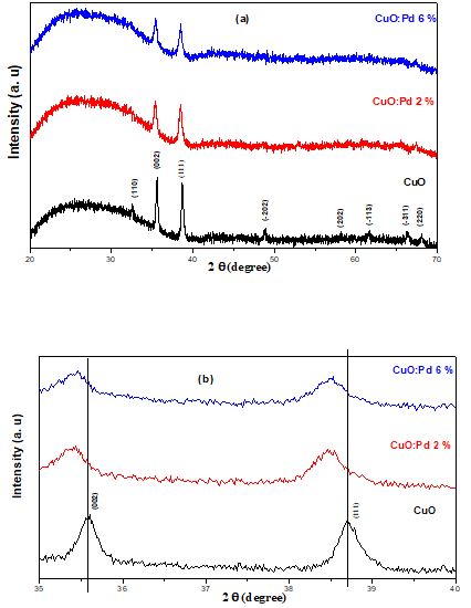
Figure 1: (a) (b) X-ray diffraction patterns for CuO, CuO: Pd 2%, and CuO: Pd 6% thin films
FIGURE 2
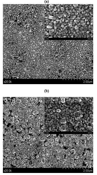
FIGURE 3
Figure 2: SEM images of CuO and Pd-doped CuO thin films as a function of Pd doping: (a) 0%, (b) 2% and (c) 6%
FIGURE 4
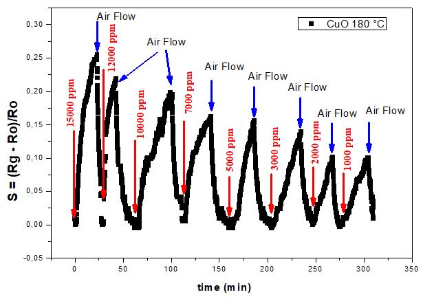
Figure 3: Response of the undoped CuO sensor to hydrogen at 180 °C operating temperature, for the hydrogen concentration range 15 000 – 1000 ppm.
FIGURE 5
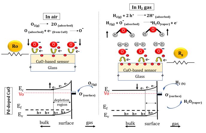
Figure 4: Illustration of hydrogen sensing mechanism of by CuO-based sensor and relevant energy band diagram
FIGURE 6
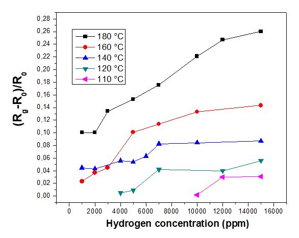
Figure 5: Sensor response of undoped CuO with respect to hydrogen concentration for various operating temperatures
FIGURE 7
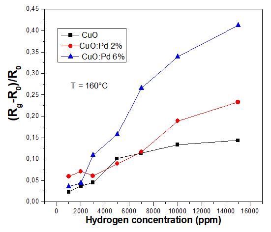
Figure 6: Maximum response of CuO, CuO: Pd 2% and CuO: Pd 6% sensors to different hydrogen concentrations for an operating temperature of 160 °C
FIGURE 8
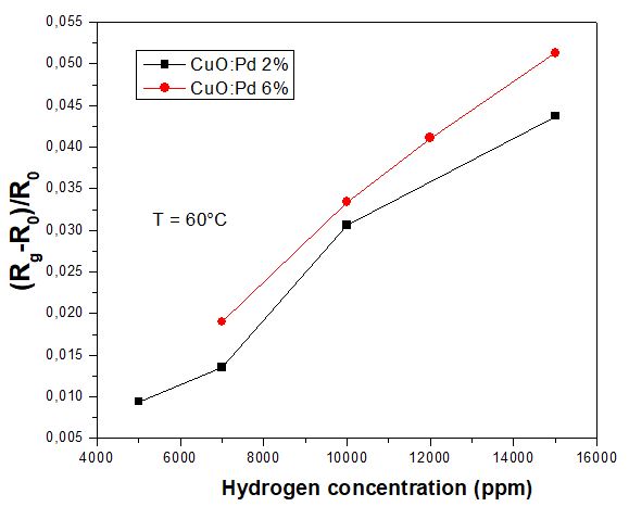
Figure 7: Comparison of the response of the sensors CuO: Pd 2% and CuO: Pd 6% to different hydrogen concentrations at 60°C
Tables at a glance
Figures at a glance