Figure 1 (a) Propagation of Surface Plasmon Polaritons (SPP), and (b) Oscillation of Localized Surface Plasmons (LSP) [2]. Reproduced with permission from Nature Photonics 5, 349–356 (2011), Nature Publishing Group.

Figure 1 (a) Propagation of Surface Plasmon Polaritons (SPP), and (b) Oscillation of Localized Surface Plasmons (LSP) [2]. Reproduced with permission from Nature Photonics 5, 349–356 (2011), Nature Publishing Group.
Figure 2 The fluorescence peak of CdSe with different size of quantum dots. Magnitude of intensity spectrum doesn’t depend on the size of quantum dots but its operating wavelength changes with the dimension of the quantum dots. Spectrum shifts towards higher frequency (blue shift) as its dimension reduces [5]. Reprinted from book of Adv in Biomedical Eng, Vol 9 (2012), IERI. (Open Access)
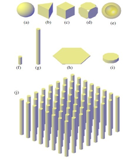
Figure 3 Schematic of metal nanostructures: (a) nanosphere, (b)nanoprism, (c) nanocube, (d) nanocage, (e) nanoshell, (f) nanorod, (g) nanowire,(h) nanosheet, (i) nanodisk, and (j) nanowire array.Reproduced with permission from Advances in Optics and Photonics, Vol. 4, Issue 2, pp. 157-321 (2012), OSA[6]
Figure 4 Absorption spectrum ofvarioussizesandshapes of gold nanoparticles. Absorption spectra doesn’t change significantly with the size of nanospheres while for nanorods as the aspect ratio (AR) increases corresponding spectra moves towards higher wavelength. Higher the AR larger the spectrum bandwidth, greater the sensitivity [43].Reproduced with permission from Chemical Society Reviews.,35, 209-217 (2006), Royal Society of Chemistry.
Figure 5 (a) Electromagnetic interactionwith metalnanosphere. (b) Transversal resonance modeand (c) longitudinal resonance mode for LSPsin a metal nanosphere. Reproduced with permission from Langmuir 22(1), 32–41 (2006),American Chemical Society. [44].
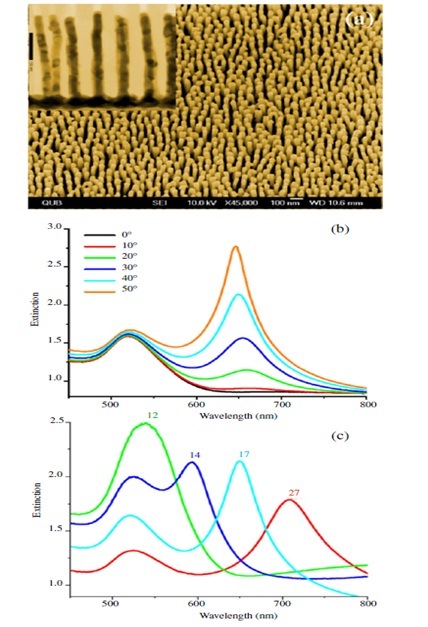
Figure 6 (a) SEM image of Au nanorods in air. Inset, TEM image of Au nanorods in anodic aluminium oxide (AAO). (b) Zero-order opticalextinction spectra for different of incidence angles. The nanorod length is300 nm, diameter is 30 nm, and the interrod distance is about 100 nm. (c)Zero-order optical extinction spectra of Au nanorods in AAO as afunction of rod aspect ratio. The nanorod length is 400 nm and the interred distance is about 100 nm. The plots are labeled according to the nanorod’s aspectratio, corresponding to the diameters from about 15 to 30 nm.Reproduced with permission from Opt. Express16(10), 7460–7470 (2008), OSA [45].
Figure 7 Experimental extinction spectrum of a concentric nanoshell particle(solid curve) and the theoretical extinction spectrum (dashed curve) calculatedby using various dielectric values for gold. The variousorder multipoles of the plasmon are plotted separately (dotted curves).Reproducedwith permission from Nano Lett.4(7), 1323–1327 (2004). [50].
Figure 8 (a) Schematic view of two weakly coupled oscillatorsand a driving force (b) dependence of resonance characteristic on the amplitude of the forced oscillator |c1|, and (c) resonance characteristic coupled to |c2|. There are two resonances for these weakly coupled oscillators. The forced oscillator (ω1, C1) exhibits resonances with symmetricand asymmetric profiles for eigenfrequencies ω1 =1 and ω2=1.2 (b), respectively. The second coupled oscillatorexhibits symmetric resonant profiles only (c). Reproducedwith permission fromRev. Mod. Phys. 82(3), 2257–2298 (2010), APS [51]
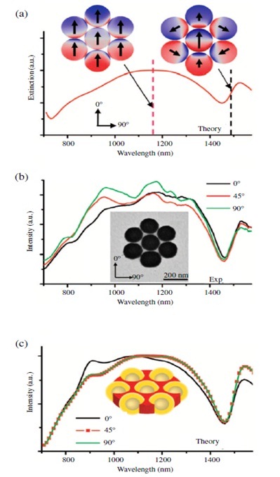
Figure 9 Fano-resonance characteristic of a plasmonicheptamer. (a) Calculated extinctionspectrum and charge density plots for a heptamer excited at normal incidence.The nanoshells have dimensions [r1, r2]=[62.5, 85] nm, and the clusterhas 1.6 nm gap separations and is embedded in a cylinder with a dielectricconstant ε = 2.5. The Fano minimum is at 1450 nm. The charge density plotof the heptamer is at 1490 nm. (b) TEM image and spectra of a heptamerat three different incident electric-field orientation angles. The nanoshells aremeasured to have average dimensions [r1, r2]=[62.5, 85] nm. The Fanominimum at 1450 nm is isotropic for these orientation angles. (c) Calculatedscattering spectra for a heptamer with a geometry matching that in (a), forthe three orientation angles in (b). Reproduced with permission from Science 328(5982), 1135–1138 (2010)[53].
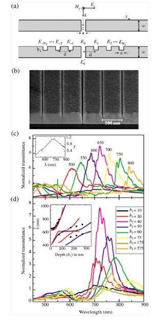
Figure 10 (a) Schematic of a single slit of width a in a metallic film of thickness w, andsingle slit symmetrically surrounded in the input surface by 2NI grooves of depthh1. The separation between adjacent indentations is d, and all groove widthsare a. (b) Electron micrograph image of one of the devices analyzed and thencross sectioned by focused-ion-beam milling. Nominal values are a = 404 nm, w = 350 nm, h1 = 100 nm, and d = 500 nm. Collection of experimentalT(λ), for different structures formed by a central slit surrounded by ±5 grooves (a = 40 nm) on the input surface of a silver film with w = 350 nm. (c)h1 = 40 nm, while the array period (d) is varied between 500 and 800 nm.The black curve corresponds to the single-slit case (also reproduced in the inset for clarity). (d) d = 650 nm, for different groove depths h1. In the inset, thespectral locations of measured transmission peaks (black dots) are comparedwith the calculated positions of the surface electromagnetic resonances of silverreflection gratings with square (blue curve) or triangular (red curve) grooves.Reproduced with permission from Phys. Rev. Lett.90(21), 213901 (2003), APS[67].
Figure 11 (a) Experimental setup for hydrogel waveguide (HW) (b) layout different surfaces and (c) reflectivity spectra for the resonant excitation HW and SP modes. Here refractive index for a hydrogel film increases ∆n_h=〖5x10〗^(-3) from index〖 n〗_h=1.345 [68].Reproduced with permission from Biosensors and Bioelectronics 25 1663–1668 (2010), Elsevier limited.
Figure 12 Resonances characteristic of different geometry and materials.a, Effects of geometry and materials on electrostatic resonances of deep-subwavelength metal nanostructures. As the surrounding dielectric constant increases the resonance for a spherical nanoparticle (shown on the left) redshifts. As the aspect ratio for a nanorod is increased the longitudinal resonance is redshifted (shown on the right). Minus (plus) signs indicate regions of high (low) electron density. b, Resonant condition (εm/εd) as a function of aspect-ratio parameter L for quasistatic spheroidal particles, which are shown in the inset. The major and minor axes of the spheroid are represented by a and b, respectively. c–e, Retardation-based strip resonators. Normalized field-intensity distributions normalized to the incident intensity for the lowest odd-order resonances of 30-nm-thick silver strips that are top-illuminated with light at wavelength of λ0 = 550 nm. E0 denotes the incident electric-field strength. Three different resonant antennas are shown that approximately measure one (c), three (d) and five (e) times λSPP/2 [69]. Reproduced with permission from Nature Materials, 9, p193-204 (2010), Nature Publishing Group.
Figure 13 Absorption spectrum of solar cell. AM1.5 solar spectrum, together with a graph that indicates the solar energy absorbed in a 2-μm-thick crystalline Si film (assuming single-pass absorption and no reflection). Clearly, a large fraction of the incident light in the spectral range 600–1,100 nm is not absorbed in a thin crystalline Si solar cell. [73]Reproduced with permission from Nature mater,9, 205-213 (2010), Nature Publishing Group.
Figure 14 Three different light-trapping techniques for thin-film solar cells.a, Light trapping by scattering from metal nanoparticles at the surface of the solar cell. Light is preferentially scattered and trapped into the semiconductor thin film by multiple and high-angle scattering, causing an increase in the effective optical path length in the cell. b, Light trapping by the excitation of localized surface plasmons in metal nanoparticles embedded in the semiconductor. The excited particles’ near-field causes the creation of electron–hole pairs in the semiconductor. c, Light trapping by the excitation of surface plasmonpolaritons at the metal/semiconductor interface. A corrugated metal back surface couples light to surface plasmonpolariton or photonic modes that propagate in the plane of the semiconductor layer [73]. Reproduced with permission from Nature mater,9, 205-213 (2010), Nature Publishing Group.
Figure 15 Optical Antenna a. transmitter b. receiver. Each antenna is used both as a receiver as well as transmitter antenna simultaneously. Reproduced with permission fromNature photonics, Vol.5, 2011 [89].
Figure 16 (a) Field energy density for a single isolated slit of 50 nm width in a 100-nm-thick aluminum film on a silicon substrate, the top-illuminated by a λ=633 nm plane wave polarized in the x direction. (b) Magnetic field distribution for the same structure [90]. Reproduced with permission from Optics Letters 34, 686–688 (2009), Optical Society of America.
Figure 17 (a) Plot of the absorption enhancement in a nanoscale region directly beneath a slit as a function of MDM cavity length for several widths. The FDFD simulations (symbols) show excellent agreement with the Fabry–Perot model (curves). (b) Schematic showing the relevant scattering coefficients used for the model [90]. Reproduced with permission from Optics Letters 34, 686–688 (2009), Optical Society of America.
Figure 18 Negative-index metamaterials.a, Schematic of a dye-doped double-fishnet metamaterial together with exemplary profiles of the inversion (left) and electric-field amplitude (right) at the emission wavelength (710 nm) taken at the xy-plane (top) and zx-plane (bottom). Color bars: left, light (dark) shades represent high (low) areas of inversion; right, light colors represent the local field enhancement. hm, hc and hd denote the height of the metal, cladding and dielectric layers, respectively; ax and ay are the width of the rectangular holes in the x and y direction, p is the periodicity. The incident optical pump and probe pulses are indicated by red and blue waves. b, Real and imaginary part of the extracted effective refractive indices n for different pump amplitudes. The peak electric-field amplitude of the pump increases in steps of 0.5 kV cm−1, from no pumping (cyan) to a maximum of 2.0 kV cm−1 (black). The inset shows the real and imaginary parts of the effective permeability (black and red lines, respectively) and the corresponding results of Kramers–Kronig calculations (dotted lines) for the highest peak electric-field amplitude of 2.0 kV cm−1. c, The figures-of-merit (FOM = Re{n}/Im{n}) for the same pumping amplitudes as those shown in b. d, Rate dynamics during probing in the amplifying regime of the metamaterial. Shown are the net-gain rate Γg (blue), dissipative-loss rate Γf (green), outflux/radiative-loss rate Λ (red) and energy-decay rate Γt (black). e, Dynamics of the probe–pulse intensity Is (black) and energy U inside the metamaterial (red) in the regimes of continuous excitation (CE) and free decay (FD) for the active optical metamaterial of d. [93].Reproduced with permission from Nature 11, 573-584 (2012), Nature Publishing Group.
Figure 19 Schematic layout of LRSPP-based (a) MZIM and (b) DCS. (c) Optical microscope image of the fabricated MZIM showing stripes with typical bends (curvature radius .20 mm to ensure low bend loss), 100-nmthick contact pads and connecting electrodes. (d) Magnified image of the MZIM part containing an isolating 10-µm-long break in the waveguide stripe and a part of thick electrode connected with 20-µm-long (15-nm-thin) stripe to the waveguide [98].Reproduced with permission from Applied Physics Letters.85, 5833–5835 (2004), AIP Publishing LLC.
Figure 20 Dynamic characteristics of the MZIM. Inset shows the temporal response of the MZIM measured with an offset of 2 V and a peak-to-peak voltage of 3.8 V (the electrode resistance was ,1.6 kV). Fitting exponential dependencies to the rise and fall of the MZIM output power give a response time constant of 0.7 ms [98]. Reproduced with permission from Applied Physics Letters.85, 5833–5835 (2004), AIP Publishing LLC.
Figure 21Reaction cross section is equal to the absorption cross section. a) Visible absorption cross section of a model I2 molecule near a silver sphere (a = 500 A). The molecule is perpendicular to the surface. b)Integrated absorption cross sections for the model I2 molecule perpendicular to Ag, Cu and Au spheres (a = 500 A) as a function of the molecule-surface separation. The cross sections are normalized to I when d very large [103].Reproduced with permission from Journal of Chemical Physics.75, 2205–2214 (1981), AIP Publishing LLC.